Press Release · EV Group
EV Group Helps Accelerate Qubit Scaling for Quantum Computing Through Advanced Packaging Expertise
Distributed by StarFort Tech · Originally issued via PR Newswire
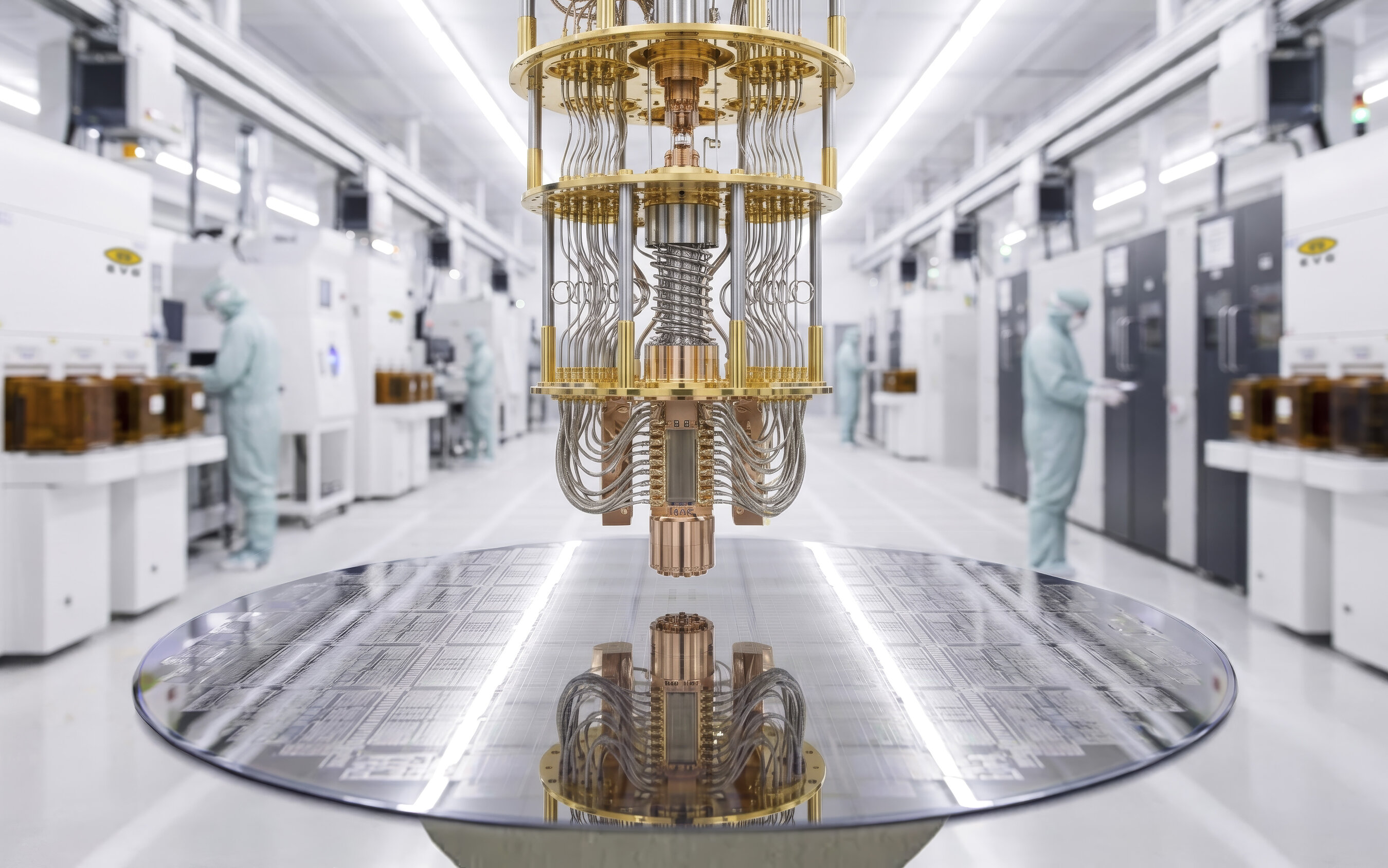
Established expertise in advanced packaging, heterogeneous integration and process development supports critical manufacturing requirements for fault-tolerant quantum computing
ST. FLORIAN, Austria, Nov. 9, 2026 — EV Group (EVG), a leading provider of innovative process solutions and expertise serving leading-edge and future semiconductor designs and chip integration schemes, today announced that it is supporting quantum chip developers and manufacturers in addressing the complex manufacturing requirements associated with scaling quantum computing systems. Building on its ongoing contributions to quantum chip development, EVG is applying its established expertise in advanced packaging, heterogeneous integration and photonics manufacturing to help customers develop and validate new product designs and manufacturing processes for increasingly complex quantum architectures.
EVG will highlight its suite of process solutions for quantum computing and other critical technologies at SEMICON Europa, the premier microelectronics and semiconductor manufacturing supply chain event in Europe, taking place this week on November 10-13 at the Messe München in Munich, Germany.
New Manufacturing Approaches Need to Scale Quantum Computing
According to McKinsey & Company, quantum computing could create up to $2.7 trillion of economic value worldwide by 2035 (1). As quantum computing advances beyond early research demonstrations toward increasingly capable systems, one of the industry's greatest challenges is scaling the number of qubits—the fundamental units of quantum information—while maintaining the performance and reliability needed for practical applications. Because qubits are extremely sensitive to errors, achieving fault-tolerant quantum computing requires significantly increasing the number of physical qubits to support error correction.
Meeting these requirements presents significant manufacturing challenges. Different quantum computing architectures rely on a wide range of materials and device structures, creating demanding requirements for high-density interconnections, heterogeneous materials integration and precision manufacturing. Advanced packaging technologies will play a key role in enabling the integration of increasingly complex quantum chips and other critical components while preserving their performance.
EVG addresses these challenges through its broad portfolio of process technologies, including fusion and hybrid bonding, high-vacuum oxide-free bonding, digital and nanoimprint lithography, and thin-wafer processing. These technologies provide the precision needed for demanding wafer alignment, bonding and patterning requirements across different quantum computing architectures. Combined with the company's materials and process integration expertise through its Heterogeneous Integration Competence Center™ (HICC) and NILPhotonics® Competence Center, these capabilities enable quantum computing companies to explore, develop and validate new quantum chip designs and manufacturing approaches.
"Quantum computing is not a single technology, but a collection of fundamentally different approaches, each with its own materials and manufacturing requirements. As developers work to scale these technologies, the challenge is not simply increasing the number of qubits but finding ways to integrate them in increasingly complex chip architectures without compromising performance," stated Dr. Bernd Dielacher, director of business development at EVG. "This is where EVG's broad portfolio of process solutions, combined with our experience in advanced packaging and heterogeneous integration, can play an important role in helping customers develop practical manufacturing solutions for a new generation of quantum devices."
Process Technologies Supporting Quantum Computing Development
Quantum computing encompasses a variety of approaches, including superconducting, photonic, spin, trapped-ion, neutral-atom and nitrogen-vacancy diamond qubits, each presenting distinct materials and manufacturing challenges. EVG's technologies address a range of manufacturing requirements across different quantum computing approaches.
For example, with superconducting quantum devices, oxide-free bonding processes can support the formation of superconducting interconnects and 3D device integration. In photonic quantum devices, fusion and oxide-free bonding enable the integration of III-V and high-Pockels-coefficient materials on waveguides, while hybrid bonding supports ultra-high-density interconnects in emerging spin qubit architectures. For trapped ion quantum computing, EVG has collaborated with researchers to develop low-temperature metal bonding processes that enable the integration of ion-trap and photonic chiplets made from different substrate materials. EVG is also a strategic partner of Silicon Austria Labs in support of the CHAMP-ION pilot line project, Europe's first open-access pilot line for industrial-scale production of ion-trap quantum chips. Additional capabilities, including nanoimprint lithography, digital lithography and temporary bonding and debonding, can support specialized optical structures and advanced packaging processes.
EVG's involvement in quantum computing development includes its recently announced collaboration with Xanadu, a developer of quantum photonic computing technology, as well as participation in research activities addressing emerging quantum device manufacturing requirements. These engagements reflect EVG's active commitment to advancing qubit integration, building on its established expertise in semiconductor and photonics manufacturing to address the specialized requirements of quantum hardware.
Meet EVG at SEMICON Europa 2026
To speak with an EVG representative and learn more about the company's industry-leading solutions for quantum computing and other critical technologies, visit EVG's booth #B1241 during exhibition hours.
Reference
(1) "McKinsey Quantum Technology Monitor 2026: A commercial tipping point," McKinsey & Company, April 28, 2026, https://www.mckinsey.com/capabilities/mckinsey-technology/our-insights/mckinsey-quantum-technology-monitor-2026-a-commercial-tipping-point
SOURCE EV Group
About EV Group (EVG)
EV Group (EVG) provides innovative process solutions and expertise that serve leading-edge and future semiconductor designs and chip integration schemes. The company's vision of being the first in exploring new techniques and supporting next-generation applications of micro- and nanofabrication technologies enables customers to successfully commercialize new product ideas. EVG's high-volume-manufacturing-ready products, which include wafer bonding, lithography, thin-wafer processing and metrology equipment, enable advances in semiconductor front-end scaling, 3D integration and advanced packaging, as well as in other electronics and photonics applications. More information about EVG is available at www.EVGroup.com.